Doppler Broadening Spectroscopy (DBS)
Doppler Broadening Spectroscopy (DBS) is a powerful positron-based technique used to study the electronic structure and defects in materials. It is complementary to Positron Annihilation Lifetime Spectroscopy (PALS) and focuses on the energy distribution of gamma rays produced during positron–electron annihilation.
While PALS provides information about how long positrons survive inside a material, DBS reveals where and how they annihilate—that is, the momentum of the electrons involved in the annihilation process. This makes DBS particularly useful for identifying vacancy-type defects, impurities, and chemical surroundings at the atomic level.
Basic Principle
When a positron encounters an electron, they annihilate and emit two gamma photons, each with an ideal energy of 511 keV.
However, because electrons inside atoms have their own momenta, these photons are not emitted at exactly 511 keV. Instead, their energies are slightly shifted — one slightly above and the other slightly below this value.
This small Doppler shift depends on the momentum of the annihilating electron.
By precisely measuring this energy broadening around 511 keV, we can obtain detailed information about the electron momentum distribution at the annihilation site.
Experimental Setup
A typical DBS system consists of:
-
A positron source (often Sodium-22),
-
A high-resolution gamma-ray detector,
-
A multichannel analyzer (MCA) for recording the energy spectrum.
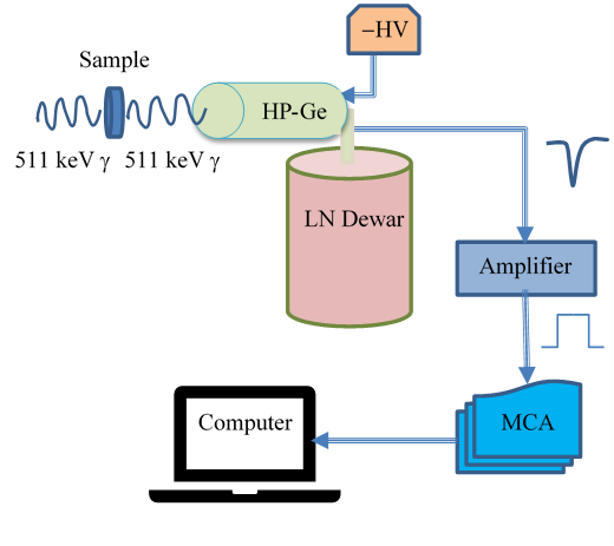
The positron source is placed between two thin samples or on the surface of the material under study. The emitted positrons penetrate the sample, thermalize, and eventually annihilate with electrons.
The detector measures the energy of the resulting gamma photons with extremely high precision—often using high-purity germanium (HPGe) or semiconductor detectors, capable of resolving energy differences smaller than 1 keV near 511 keV.
Energy Spectrum and S–W Parameters
The recorded gamma-ray spectrum shows a sharp peak centered at 511 keV. The shape of this peak carries information about the annihilation environment:
-
The S-parameter (shape parameter):
Represents the fraction of counts in the central region of the 511 keV peak.
A higher S-value corresponds to annihilation with low-momentum valence electrons, often associated with open-volume defects such as vacancies or voids. -
The W-parameter (wing parameter):
Represents the fraction of counts in the “wings” or outer regions of the peak.
Higher W-values indicate annihilation with high-momentum core electrons, which are more localized around atomic nuclei.
By plotting S and W together (the S–W correlation plot), researchers can distinguish between different defect types or chemical environments, since each produces a unique signature.
Depth Profiling with Variable-Energy Beams
In advanced DBS systems, such as variable-energy positron beam setups, the positron implantation energy can be precisely controlled from a few hundred eV to tens of keV.
Lower energies probe surface or near-surface regions, while higher energies reach deeper layers (up to several micrometers).
This makes DBS a powerful non-destructive tool for analyzing thin films, interfaces, coatings, and semiconductor junctions in three dimensions.
Data Interpretation
-
High S / Low W: Indicates large open-volume defects (e.g., vacancies, voids, or free volume in polymers).
-
Low S / High W: Indicates annihilation in dense regions or near heavy atoms with high core electron momentum.
-
Linear trends in S–W plots often correspond to mixtures of two annihilation states (e.g., bulk + defect).
Combined with PALS, DBS provides a comprehensive picture: PALS measures the defect size, while DBS reveals the defect’s chemical and electronic nature.
Summary
Doppler Broadening Spectroscopy allows scientists to “see” the electronic fingerprints of atomic-scale defects.
By analyzing the broadening of the 511 keV annihilation line, DBS reveals whether positrons annihilate in perfect lattice sites, open-volume defects, or near specific atomic species.
Because of its sensitivity, depth resolution, and non-destructive nature, DBS is an essential technique in materials science, semiconductor physics, and surface/interface studies, often used alongside PALS in modern positron laboratories.
This page updated by Pozitron/Pozitronyum Araştırma ve Hizmet Laboratuvarı on 02.11.2025 18:27:55


